Image may be NSFW.
Clik here to view.
The next big leap in computing, chips based on microscopic three dimensional transistors, designed by "socialist Berkeley radical professor" Chenming Hu, will be used in all of Intel's next generation of chips. The new chips with 3D technology will use half the power, and have double the transistor density, of today's fastest chips. Chip miniaturization, faster speed and low power demand will be the basis for a new advanced generation of hand held devices and computers. Because it draws less power, this transistor design is both more environmentally friendly and better for battery powered portable devices. Moreover, the small additional cost of production of the 3D chip will be paid back many times over by reduced power costs.
This engine of economic growth will be based on technology developed under a federal government grant at U.C. Berkeley, by a professor who took the radical step of giving away his work for free.
"I have patented things in the past but in this case we feel it's best to make it as widely available as possible," Hu explained. Hu, who has also released software under open source licenses, said he was confident the industry will adopt the technology.
Yes, technology that will add significantly to global economic growth is open source. The key to Professor Hu's success was a stable academic environment, not a huge salary and benefits package. Republicans who attack public universities such as Berkeley are attacking America's future. Federally funded university research is one of the major engines of American economic growth.
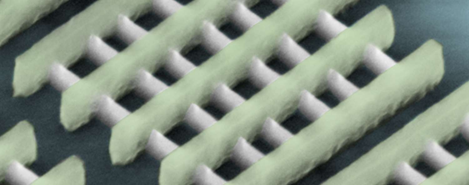
The new transistor design uses a "fin" for the current conducting channel. Because the fin can be controlled in 3 dimensions by electric fields less power leaks across the gate when it is off. The old transistor design cannot be made smaller than 32nm because the gate is already leaking a large percentage of current. Two dimensional transistor design had reached its physical limit.
Image may be NSFW.
Clik here to view. Source: Intel An illustration of a 32nm transistor compared to a 22nm transistor. On the left side is the 32nm planar transistor in which the current (represented by the yellow dots) flows in a plane underneath the gate. On the right is the 22nm 3-D Tri-Gate transistor with current flowing on 3 sides of a vertical fin.
This creative technological breakthrough wasn't made by an executive with a seven or eight figure compensation package. It was made by a public university professor who has been recognized for excellence in teaching.
These three-dimensional transistors were first imagined and built by three researchers at the University of California, Berkeley, in the late 1990s, in response to a call from the United States Defense Advanced Research Projects Agency for designs that would allow transistors to scale below 25 nanometers, an order of magnitude smaller than the ones in production at the time. Chenming Hu wrote out the technical specs for the new transistor on a plane ride to Japan in 1996. A Berkeley group made up of Hu, Jeffrey Bokor, and Tsu-Jae King Liu first made these transistors, which they called FinFETs, in 1999."It was an instant hit," says Hu. The university opted to release the intellectual property into the public domain instead of patenting it; as the Berkeley researchers kept refining the designs, Hu presented the work at several companies, including Intel. By 2002, the FinFET and a second Berkeley design, known as "silicon on insulator," were the devices favored by the International Technology Roadmap of Semiconductors as the technologies likely to meet the industry's needs in the next 15 years. But at Intel, at least, FinFET pulled ahead of the second design, which relies on adding a very thin layer of silicon to a transistor. Until about two years ago, the companies who make silicon wafers weren't able to make the active layer thin enough. French company Soitec can now manufacture the necessary wafers for this alternate design, and Hu says Intel's competitors may at some point adopt it.